ADN2817
The ADN2817/ADN2818 provide the receiver functions of quantization, signal level detect, and clock and data recovery for continuous data rates from 10 Mbps to 2.7 Gbps. The ADN2817/ ADN2818 automatically lock to all data rates without the need for an external reference clock or programming. All SONET jitter requirements are exceeded, including jitter transfer, jitter generation, and jitter tolerance. All specifications are quoted for -40°C to +85°C ambient temperature, unless otherwise noted.
This device, together with a PIN diode and a TIA preamplifier, can implement a highly integrated, low cost, and low power fiber optic receiver.
The ADN2817/ADN2818 have many optional features available through an I^2C(R) interface. For example, the user can read back the data rate onto which the ADN2817 or ADN2818 is locked, or the user can set the device to lock only to one particular data rate if provisioning of data rates is required. A BERMON circuit provides an estimate of the received bit error rate (BER) without interruption of the data. Alternatively, the user can adjust the data sampling phase to optimize the received BER.
The ADN2817/ADN2818 are available in a compact 5 mm × 5 mm, 32-lead, lead frame chip scale package.
产品应用领域 Applications
- SONET OC-1, OC-3, OC-12, OC-48, and all associated FEC rates
- Fibre Channel, 2× Fibre Channel, GbE, HDTV, and others
- WDM transponders
- Regenerators/repeaters
- Test equipment
ADN2817 特点
- Serial data input: 10 Mbps to 2.7 Gbps
- Exceeds ITU-T jitter specifications
- Integrated limiting amplifier 5 mV sensitivity (ADN2817 only)
- Adjustable slice level: ±100 mV (ADN2817 only)
- Patented dual-loop clock recovery architecture
- Programmable LOS detect (ADN2817 only)
- Integrated PRBS generator and detector
- See Data Sheet for Additional Information
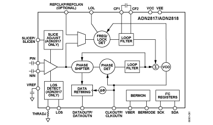
ADN2817 功能框图
| 产品型号 | 产品状态 | 封装 | 引脚 | 温度范围 |
|---|---|---|---|---|
| ADN2817ACPZ | 量产 | 32 ld LFCSP (5x5mm CP-32-2) | 32 | 商业 |
| ADN2817ACPZ-RL | 量产 | 32 ld LFCSP (5x5mm CP-32-2) | 32 | 工业 |
| ADN2817ACPZ-RL7 | 量产 | 32 ld LFCSP (5x5mm CP-32-2) | 32 | 工业 |
| EVAL-ADN2817EBZ | 量产 | 评估板 | - | 工业 |