ADN2807: 155/622 Mb/s Clock and Data Recovery IC with Integrated Limiting Amp
The ADN2807 provides the receiver functions of quantization, signal level detect, and clock and data recovery at rates of OC-3, OC-12, and 15/14 FEC. All SONET jitter requirements are met, including jitter transfer, jitter generation, and jitter tolerance. All specifications are quoted for –40°C to +85°C ambient temperature, unless otherwise noted. The device is intended for WDM system applications and can be used with either an external reference clock or an on-chip oscillator with external crystal. Both native rates and 15/14 rate digital wrappers are supported by the ADN2807, without any change of reference clock. This device, together with a PIN diode and a TIA preamplifier, can implement a highly integrated, low cost, low power, fiber optic receiver. The receiver front end signal detect circuit indicates when the input signal level has fallen below a user adjustable threshold. The signal detect circuit has hysteresis to prevent chatter at the output. The ADN2807 is available in a compact 7 mm × 7 mm 48-lead chip-scale package (LFCSP).
ADN2807 特点
- Meets SONET requirements for jitter transfer/ generation/tolerance
- Quantizer sensitivity: 4 mV typical
- Adjustable slice level: ±100 mV
- Patented clock recovery architecture
- Loss-of-signal detect range: 3 mV to 15 mV
- Loss-of-lock indicator
- Single-reference clock frequency for all rates, including 15/14 (7%) wrapper rate
- Output squelch and bypass features
- Single-supply operation: 3.3 V
- Low power: 540 mW typical
- 7 mm × 7 mm 48-lead LFCSP
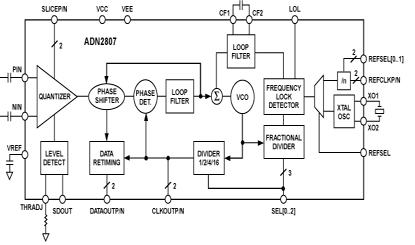
ADN2807 功能框图
| 产品型号 | 产品状态 | 封装 | 引脚 | 温度范围 |
|---|---|---|---|---|
| ADN2807ACP | 量产 | 48 ld LFCSP 7x7mm (5.25EP) | 48 | 商业 |
| ADN2807ACPZ | 量产 | 48 ld LFCSP 7x7mm (5.25EP) | 48 | 商业 |
| ADN2807ACPZ-RL | 量产 | 48 ld LFCSP 7x7mm (5.25EP) | 48 | 商业 |
| EVAL-ADN2807-CML | 量产 | 评估板 | - | 待定 |