ADL5519: 对数放大器和检测器
The ADL5519 is a dual-demodulating logarithmic amplifier that incorporates two AD8317s. It can accurately convert an RF input signal into a corresponding decibel-scaled output. The ADL5519 provides accurately scaled, independent, logarithmic output voltages for both RF measurement channels. The device has two additional output ports, OUTP and OUTN, that provide the measured differences between the OUTA and OUTB channels. The on-chip channel matching makes the log amp outputs insensitive to temperature and process variations.
The temperature sensor pin provides a scaled voltage that is proportional to the temperature over the operating temperature range of the device.
The ADL5519 maintains accurate log conformance for signals from 1 MHz to 8 GHz and provides useful operation to 10 GHz. The ±3 dB dynamic range is typically 62 dB and has a ±1 dB dynamic range of >50 dB (re: 50 Ω). The ADL5519 has a response time of 6 ns/8 ns (fall time/rise time) that enables RF burst detection to a pulse rate of greater than 50 MHz. The device provides unprecedented logarithmic intercept stability vs. ambient temperature conditions. A supply of 3.3 V to 5.5 V is required to power the device. Current consumption is typically 60 mA, and it decreases to less than 1 mA when the device is disabled.
The device is capable of supplying four log amp measurements simultaneously. Linear-in-dB measurements are provided at OUTA and OUTB with conveniently scaled slopes of -22 mV/dB. The log amp difference between OUTA and OUTB is available as differential or single-ended signals at OUTP and OUTN. An optional voltage applied to VLVL provides a common-mode reference level to offset OUTP and OUTN above ground. The broadband output pins can support many system solutions.
Any of the ADL5519 output pins can be configured to provide a control voltage to a variable gain amplifier (VGA). Special attention has been paid to minimize the broadband noise of the output pins so that they can be used for controller applications.
The ADL5519 is fabricated on a SiGe bipolar IC process and is available in a 5 mm × 5 mm, 32-lead LFCSP with an operating temperature range of -40°C to +125°C.
产品应用领域 Applications
- RF transmitter power amplifier linearization and gain/power control
- Power monitoring in radio link transmitters
- Dual-channel wireless infrastructure radios
- Antenna VSWR monitor
- RSSI measurement in base stations, WLAN, WiMAX, radar
ADL5519 特点
- Wide bandwidth: 1 MHz to 10 GHz
- Dual-channel and channel difference output ports
- Integrated accurate scaled temperature sensor
- 62 dB dynamic range (±3 dB)
- >50 dB with ±1 dB up to 8 GHz
- Stability over temperature: ±0.5 dB (-40oC to +85oC)
- Low noise detector/controller outputs
- Pulse response time: 6 ns/8 ns (fall time/rise time)
- Supply operation: 3.3 V to 5.5 V @ 60 mA
- Fabricated using high speed SiGe process
- Small footprint, 5 mm × 5 mm, 32-lead LFCSP
- Operating temperature range: -40°C to +125°C
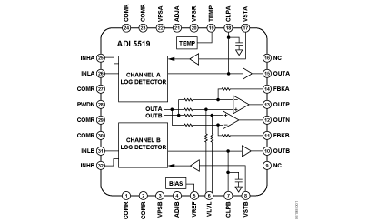
ADL5519 功能框图
AD8311 功能框图
ADL5519 技术指标
| RF Frequency (MHz) | 1 kHz to 10000 | Response Time (ns typ) | 6ns |
| Dynamic Range (dB) | 62dB | Voltage Supply (V) | 3 to 5.5 |
| Temp Stability (dB) | ±0.5dB | Supply Current | 56mA |
| Package | 32-Lead LFCSP |
ADL5519 订购指南
| 产品型号 | 产品状态 | 封装 | 引脚 | 温度范围 |
|---|---|---|---|---|
| ADL5519-EVALZ | 量产 | 评估板 | 24 | 汽车级 |
| ADL5519ACPZ-R2 | 量产 | 32 ld LFCSP (5x5x.85mm) w/2.7exposed pad | 32 | 汽车级 |
| ADL5519ACPZ-R7 | 量产 | 32 ld LFCSP (5x5x.85mm) w/2.7exposed pad | 32 | 汽车级 |
| ADL5519ACPZ-WP | 量产 | 32 ld LFCSP (5x5x.85mm) w/2.7exposed pad | 32 | 汽车级 |