ADF4193: Low Phase Noise, Fast Settling PLL
The ADF4193 frequency synthesizer can be used to implement local oscillators in the up-conversion and down-conversion sections of wireless receivers and transmitters. Its architecture is specifically designed to meet the GSM/EDGE lock time requirements for base stations.
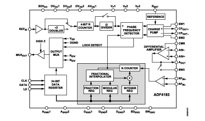
It consists of a low-noise digital phase frequency detector (PFD), and a precision differential charge pump. There is also a differential amplifier (Diff Amp) to convert the differential charge pump output to a single ended voltage for the external voltage controlled oscillator (VCO). The Σ-Δ based fractional interpolator, working with the N divider, allow programmable modulus fractional-N division. Additionally, the 4-bit reference (R) counter and on-chip frequency doubler, allows selectable reference signal (REFIN) frequencies at the PFD input.
A complete phase-locked loop (PLL) can be implemented if the synthesizer is used with an external loop filter and a VCO. The switching architecture ensures that the PLL settles inside the GSM time slot guard period, removing the need for a second PLL and associated isolation switches. This saves cost, complexity, PCB area, shielding and characterization on previous ping-pong GSM PLL architectures.
ADF4193 特点
- New fast settling fractional-N PLL architecture
- Frequency hop across the GSM band in 5 us, phase settled by 20 us
- Single PLL replaces ping-pong synthesizers
- 0.5 degree RMS phase error at 2 GHz RF output
- Digitally programmable output phase
- RF input range up to 3.5 GHz
- On-chip low noise differential amplifier
- Phase noise figure of merit –216 dBc/Hz
- Loop filter design possible using ADI SimPLL
ADF4193 功能框图
| 产品型号 | 产品状态 | 封装 | 引脚 | 温度范围 |
|---|---|---|---|---|
| ADF4193BCPZ | 量产 | 32 ld LFCSP (5x5mm) w/3.3mm exposed pad | 32 | 商业 |
| ADF4193BCPZ-RL | 量产 | 32 ld LFCSP (5x5mm) w/3.3mm exposed pad | 32 | 商业 |
| ADF4193BCPZ-RL7 | 量产 | 32 ld LFCSP (5x5mm) w/3.3mm exposed pad | 32 | 商业 |
| EVAL-ADF4193EBZ1 | 量产 | 评估板 | - | 待定 |
| EVAL-ADF4193EBZ2 | 量产 | 评估板 | - | 待定 |
ADF4193 应用技术支持与电子电路设计开发资源下载
- ADF4193 数据手册DataSheet 下载 . PDF
- ADI 模拟器件公司比较器产品选型指南 . PDF
- Analog Devices, Inc. 美国模拟器件公司产品订购手册 .PDF
- 时钟和定时IC产品介绍 . PDF