ADADC80: 12-Bit Successive-Approximation Integrated Circuit ADC
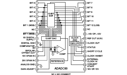
The ADADC80* is a complete 12-bit successive-approximation analog-to-digital converter (ADC) that includes an internal clock, reference, and comparator. Its hybrid IC design uses MSI digital and linear monolithic chips in conjunction with a 12-bit monolithic digital-to-analog converter (DAC) to provide modular performance and versatility with IC size, price, and reliability.
Important performance characteristics of the ADADC80 include a maximum linearity error of ±0.012% at 25°C, maximum gain TC of 30 ppm/°C, typical power dissipation of 800 mW, and maximum conversion time of 25 μs. Monotonic operation of the feedback DAC guarantees no missing codes over the temperature range of -25°C to +85°C.
The design of the ADADC80 includes scaling resistors that provide an analog signal range of ±2.5 V, ±5.0 V, ±10 V, 0 V to +5.0 V, or 0 V to +10.0 V. The 6.3 V precision reference can be used for external applications. All digital signals are fully DTL and TTL compatible; output data is in parallel form.
The ADADC80 is available in grades specified for use over the -25°C to +85°C temperature range and is available in a 32-lead ceramic DIP.
产品焦点 Product Highlights
- The ADADC80 is a complete 12-bit ADC. No external components are required to perform a conversion.
- A monolithic 12-bit feedback DAC is used for reduced chip count and higher reliability.
- The internal buried Zener reference is laser trimmed to 6.3 V. The reference voltage is available externally and can supply up to 1.5 mA beyond the current required for the reference and bipolar offset.
- The scaling resistors are included on the monolithic DAC for exceptional thermal tracking.
- The ADADC80 directly replaces other devices of this type, providing significant increases in performance.
- The fast conversion rate of the ADADC80 makes it an excellent choice for applications requiring high system throughput rates.
- The short cycle and external clock options are provided for applications requiring faster conversion speed or lower resolution.
ADADC80 特点
- True 12-bit operation: max nonlinearity ±0.012%
- Low gain temperature coefficient (TC): ±30 ppm/°C maximum
- Low Power: 800 mW
- Fast conversion time: 25 us
- Precision 6.3 V reference for external application
- Short-cycle capability
- Parallel data output
- See Data Sheet for Additional Information
ADADC80 功能框图
| 产品型号 | 产品状态 | 封装 | 引脚 | 温度范围 |
|---|---|---|---|---|
| ADADC80-12 | Prodn | 32 ld Side Brazed CerDip (41.05x23.11) | 32 | Ind |
| ADADC80-Z-12 | Prodn | 32 ld Side Brazed CerDip (41.05x23.11) | 32 | Ind |