AD9515: 1.6 GHz Clock Distribution IC, Dividers, Delay Adjust, Two Outputs
The AD9515 features a two-output clock distribution IC in a design that emphasizes low jitter and phase noise to maximize data converter performance. Other applications with demanding phase noise and jitter requirements also benefit from this part.
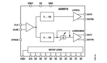
There are two independent clock outputs. One output is LVPECL, while the other output can be set to either LVDS or CMOS levels. The LVPECL output operates to 1.6 GHz. The other output operates to 800 MHz in LVDS mode and to 250 MHz in CMOS mode.
Each output has a programmable divider that can be set to divide by a selected set of integers ranging from 1 to 32. The phase of one clock output relative to the other clock output can be set by means of a divider phase select function that serves as a coarse timing adjustment.
The LVDS/CMOS output features a delay element with three selectable full-scale delay values (1.5 ns, 5 ns, and 10 ns), each with 16 steps of fine adjustment.
The AD9515 does not require an external controller for operation or setup. The device is programmed by means of 11 pins (S0 to S10) using 4-level logic. The programming pins are internally biased to 1/3 VS. The VREF pin provides a level of 2/3 VS. VS (3.3 V) and GND (0 V) provide the other two logic levels.
The AD9515 is ideally suited for data converter clocking applications where maximum converter performance is achieved by encode signals with subpicosecond jitter.
The AD9515 is available in a 32-lead LFCSP and operates from a single 3.3 V supply. The temperature range is -40°C to +85°C.
产品应用领域 Applications
- Low jitter, low phase noise clock distribution
- Clocking high speed ADC, DAC, DDS, DDC, DUC, MxFE
- High performance wireless transceivers
- High performance instrumentation
- Broadband infrastructure
- ATE
AD9515 特点
- 1.6 GHz differential clock input
- 2 programmable dividers, in range from
1 to 32
Phase select for output-to-output coarse delay adjust - 1.6 GHz LVPECL clock output
LVPECL Additive output jitter 225 fs rms - 800 MHz/250 MHz LVDS/CMOS clock output
LVDS/CMOS Additive output jitter 300 fs rms/290 fs rms
Time delays up to 10 ns - Device configured with 4-level logic pins
- Space-saving, 32-lead LFCSP
AD9515 功能框图
| 产品型号 | 产品状态 | 封装 | 引脚 | 温度范围 |
|---|---|---|---|---|
| AD9515/PCBZ | 量产 | 评估板 | - | 商业 |
| AD9515BCPZ | 量产 | 32 ld LFCSP (5x5mm CP-32-2) | 32 | 工业 |
| AD9515BCPZ-REEL7 | 量产 | 32 ld LFCSP (5x5mm CP-32-2) | 32 | 工业 |
AD9515 应用技术支持与电子电路设计开发资源下载
- AD9515 数据手册DataSheet 下载 . PDF
- ADI 模拟器件公司比较器产品选型指南 . PDF
- Analog Devices, Inc. 美国模拟器件公司产品订购手册 .PDF
- 时钟和定时IC产品介绍 . PDF