AD9510: 1.2 GHz Clock Distribution IC, PLL Core, Dividers, Delay Adjust, Eight Outputs
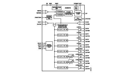
The AD9510 provides a multi-output clock distribution function along with an on-chip PLL core. The design emphasizes low jitter and low phase noise in order to maximize data converter clocking performance. Four independent LVPECL and four LVDS clock outputs operate to 1.2 GHz and 800 MHz respectively. Optional CMOS clock outputs available to 250 MHz.
The PLL section consists of a programmable reference divider, R; a low-noise phase frequency detector, PFD; a precision charge pump, CP; and a programmable feedback divider, N. By connecting an external VCXO or VCO to the CLK2 and CLK2B pins, PLL output frequencies up to 1.6 GHz may be synchronized to the input reference, REFIN.
The clock distribution section provides LVPECL outputs and outputs that may be programmed to either LVDS or CMOS. Each output has a programmable divider, which may be bypassed or set to divide by any integer up to 32.
Each divider allows the user to change the phase of one clock output relative to another clock output. This phase select functions as a coarse timing adjustment. Some outputs also feature programmable delay elements with a user-selected, fullscale range to 10 ns. This fine tuning delay block is programmed with a 5-bit word, which gives the user 32 possible delays from which to choose.
The AD9510 is ideally suited for data converter clocking applications where maximum converter performance is achieved with sub-picosecond jitter encode signals.
The AD9510 is available in a 64-lead LFCSP and is specified from -40°C to +85°C. The part may be run from a single 3.3 V supply. Users wishing to extend the voltage range for external VCOs may run the charge pump supply, VCP, to 5.5V.
AD9510 特点
- Low jitter, low phase noise clock distribution
- Clocking high speed ADCs, DACs, DDS, DDC, DUC, MxFETM Converters
- Wireless infrastructure transceivers
- High performance instrumentation
- Broadband infrastructure
AD9510 功能框图
AD9510 芯片订购指南| 产品型号 | 产品状态 | 封装 | 引脚 | 温度范围 |
|---|---|---|---|---|
| AD9510-VCO/PCB | 量产 | 评估板 | 64 | 商业 |
| AD9510-VCO/PCBZ | 量产 | 评估板 | 64 | 商业 |
| AD9510/PCBZ | 量产 | 评估板 | 64 | 商业 |
| AD9510BCPZ | 量产 | 64 ld LFCSP (9x9mm, 4.70mm exposed pad) | 64 | 工业 |
| AD9510BCPZ-REEL7 | 量产 | 64 ld LFCSP (9x9mm, 4.70mm exposed pad) | 64 | 工业 |
AD9510 应用技术支持与电子电路设计开发资源下载
- AD9510 数据手册DataSheet 下载 . PDF
- ADI 模拟器件公司比较器产品选型指南 . PDF
- Analog Devices, Inc. 美国模拟器件公司产品订购手册 .PDF
- 时钟和定时IC产品介绍 . PDF
