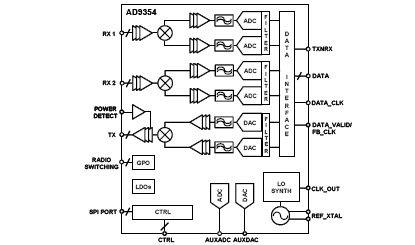
AD9354: WiMAX/WiBRO RF MxFETM MISO Transceiver
The AD9354 is a radio frequency (RF) transceiver with a single transmitter and dual receivers fully integrated into the device. This allows the part to be used for mobile and fixed WiMAX/WiBro wireless network systems. By incorporating an RF MxFETM, the AD9354 offers the combination of an RF front end and a mixed-signal baseband, enabling an easy-to-use JESD-207-compliant digital interface to the baseband application-specific integrated circuit (ASIC) or field-programmable gate array (FPGA). In addition, the AD9354 operates in the 2.3 GHz to 2.7 GHz range, covering most of the licensed and unlicensed bands. Channel bandwidths of 3.5 MHz, 4.375 MHz, 5 MHz, 7 MHz, 8.75 MHz, and 10 MHz are supported.
The direct-conversion receivers have state-of-the-art noise figure (NF) and linearity and, with the exception of baluns, do not require external components. The complete RF subsystem integrates autonomous automatic gain control (AGC) loops and dc offset corrections, thus eliminating the need for high speed interaction with the baseband processor.
The received signal is digitized with a set of four analog-to-digital converters (ADCs) with high dynamic range. Decimation and channel filters produce a 10-bit output signal at the appropriate sample rate determined by the bandwidth mode. The transmit path interpolates 10-bit input data before converting it to the analog domain, and then upconverting it to the carrier frequency.
The highly linear transmit path has excellent spectral purity with sideband noise less than -134 dBm/Hz at 22 MHz offset, and it offers an error vector magnitude (EVM) of -38 dB. The transmit power is detected by an accurate power detector with a range of more than 40 dB and 0.5 dB steps. The output power can be calibrated at the factory by a single measurement.
The reference frequency is produced by an internal digitally controlled crystal oscillator (DCXO) that has a programmable frequency offset correction with a resolution of 0.012 ppm, thus reducing the total bill of materials (BOM) of the device.
An internal auxiliary ADC and an auxiliary digital-to-analog converter (DAC) are available for system monitoring and control. Four general-purpose I/Os are also included and can be register programmed or automatically sequenced by a user-defined state machine. Mode control is via a 3- or 4-wire serial port and four real-time I/O control pins. The AD9354 is powered either from a single 3.3 V supply or, for power savings, from dual supplies and contains on-chip low dropout (LDO) regulators. The AD9354 is packaged in an 8 mm × 8 mm, 56-lead lead frame chip scale package (LFCSP).
AD9354 特点
- RF transceiver with integrated ADCs and DACs
- IEEE 802.16 WiMAX/ WiBRO
- Operates over the 2.3 to 2.7 GHz Band
- 3.5MHz < BW < 10MHz
- Dual Receivers, single transmitter
- Superior Receiver sensitivity with NF 3.5 dB
- Manual Rx gain or autonomous AGC mode
- Highly linear and spectrally pure transmitter
- Tx EVM = -38 dB
- Tx noise floor
< -134 dBm/Hz at fOFFSET > 22 MHz - Tx power control range of 58 dB,
resolution of 0.25 dB - Integrated fractional-N synthesizer
- 10 Hz LO step size
- LO integrated phase noise < 0.4°rms
- Automatic frequency correction < 0.012 ppm
- Industry-standard JESD-207 digital interface
AD9354 功能框图