AD9352: WiMAX/WiBro RF MxFE Transceiver
The AD9352 is a fully integrated transceiver for IEEE 802.16 WiMAX and WiBro wireless network systems. The RF MxFETM combines the RF front-end with mixed-signal baseband enabling an easy-to-use digital interface to the baseband ASIC or FPGA. The AD9352 operates in the 2.3 GHz to 2.7 GHz range covering most of the licensed and unlicensed bands. Channel bandwidths of 3.5 MHz, 4.375 MHz, 5 MHz, 7 MHz, 8.75 MHz, 10 MHz, 14 MHz, 17.5 MHz, and 20 MHz are supported.
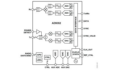
The direct-conversion receiver has state-of-the-art noise figure and linearity and requires no external components with the exception of a balun. The complete RF subsystem integrates an autonomous AGC loop and dc offset corrections, thus elimi-nating the need for high speed interaction with the baseband processor. The received signal strength indicator (RSSI) has over 80 dB of dynamic range with 0.5 dB resolution and is accessible via the serial interface.
The received signal is digitized with a high dynamic range 12-bit ADC. Decimation and channel filters produce a 10-bit output signal at the appropriate sample rate determined by the bandwidth mode. The transmit path takes a 10-bit input data and interpolates before converting to the analog domain and upconverting to the carrier frequency.
The highly linear transmit path has excellent spectral purity with sideband noise less than -134 dBc/Hz at 22 MHz offset and offers EVM of -38 dB at 0 dBm output power. The transmit power is detected by an accurate power detector and autono-mously controlled with a range of 58 dB and 0.25 dB steps. The output power can be calibrated at the factory by a single measurement.
The reference frequency is produced by an internal crystal oscillator with a digital programmable frequency with 0.012 ppm resolution thus reducing the total bill of materials of the device.
An internal auxiliary ADC and two auxiliary DACs are avail-able for system monitoring and control. Three general purpose I/Os are also included and can be register programmed or auto-matically sequenced by a user-defined state machine. Mode control is via a 4-wire serial port and four real-time I/O control pins.
The AD9352 is powered from a single 3.3 V supply and contains on-chip LDOs for each function to eliminate external regulators. The AD9352 is packaged in a 9 mm × 9 mm, 64-lead LFCSP.
产品应用领域 Applications
- WiMAX/WiBro/BWA
AD9352 特点
- RF Transceiver with Integrated ADCs and DACs
- IEEE 802.16 WiMAX/ WiBRO Systems
- Dual Band: 2.3-2.7 GHz
- 3.5MHz < BW < 20MHz
- Superior Receiver sensitivity with NF 3.7dB
- Highly linear and spectrally pure transmitter
TX EVM -38 dB
SNR > 134dB/Hz at Foffset > 22MHz - Autonomous AGC and TX Power Control
- TX power control
Range 60 dB, Resolution 0.25 dB - Automatic Frequency Correction < 0.012 ppm
- Integrated Frac-N Synthesizer
50 Hz LO step size
Integrated phase noise < 0.5°rms
AD9352 功能框图
AD9352 芯片订购指南| 产品型号 | 产品状态 | 封装 | 引脚 | 温度范围 |
|---|---|---|---|---|
| AD9352BCPZ | Prodn | 64 ld LFCSP (9x9mm, 6.20mm exposed pad) | 64 | Ind |
| AD9352BCPZ-REEL | Prodn | 64 ld LFCSP (9x9mm, 6.20mm exposed pad) | 64 | Ind |
| AD9352BCPZ-REEL7 | Prodn | 64 ld LFCSP (9x9mm, 6.20mm exposed pad) | 64 | Ind |
