AD807: 155 Mbps, Low Power, Post-Amp/Clock and Data Recovery IC
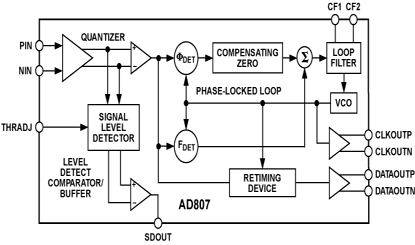
The AD807 provides the receiver functions of data quantization, signal level detect, clock recovery and data retiming for 155 Mbps NRZ data. The device, together with a PIN diode/preamplifier combination, can be used for a highly integrated, low cost, low power SONET OC-3 or SDH STM-1 fiber optic receiver.
The receiver front end signal level detect circuit indicates when the input signal level has fallen below a user adjustable threshold. The threshold is set with a single external resistor. The signal level detect circuit 3 dB optical hysteresis prevents chatter at the signal level detect output.
The PLL has a factory trimmed VCO center frequency and a frequency acquisition control loop that combine to guarantee frequency acquisition without false lock. This eliminates a reliance on external components such as a crystal or a SAW filter, to aid frequency acquisition.
The AD807 acquires frequency and phase lock on input data using two control loops that work without requiring external control. The frequency acquisition control loop initially acquires the frequency of the input data, acquiring frequency lock on random or scrambled data without the need for a preamble. At frequency lock, the frequency error is zero and the frequency detector has no further effect. The phase acquisition control loop then works to ensure that the output phase tracks the input phase. A patented phase detector has virtually eliminated pattern jitter throughout the AD807.
The device VCO uses a ring oscillator architecture and patented low noise design techniques. Jitter is 2.0 degrees rms. This low jitter results from using a fully differential signal architecture, Power Supply Rejection Ratio circuitry and a dielectrically isolated process that provides immunity from extraneous signals on the IC. The device can withstand hundreds of millivolts of power supply noise without an effect on jitter performance.
The user sets the jitter peaking and acquisition time of the PLL by choosing a damping factor capacitor whose value determines loop damping. CCITT G.958 Type A jitter transfer requirements can easily be met with a damping factor of 5 or greater.
Device design guarantees that the clock output frequency will drift by less than 20% in the absence of input data transitions. Shorting the damping factor capacitor, CD, brings the clock output frequency to the VCO center frequency.
The AD807 consumes 140 mW and operates from a single power supply at either +5 V or –5.2 V.
AD807特点
- Meets CCITT G.958 Requirements for STM-1 Regenerator-Type A
- Meets Bellcore TR-NWT-000253 Requirements for OC-3
- 155 Mbps Clock Recovery and Data Retiming
- Accepts NRZ Data, No Preamble Required
- Phase-Locked Loop Type Clock Recovery-No Crystal Required
- Quantizer Sensitivity: 2 mV
- Output Jitter: 2.0 Degrees RMS
- Level Detect Range: 2.0 mV to 30 mV
- Single Supply Operation: +5 V or –5.2 V
- Low Power: 170 mW
- 10 KH ECL/PECL Compatible Output
- Package: 16-Lead Narrow 150 mil SOIC
AD807功能框图
| 产品型号 | 产品状态 | 封装 | 引脚 | 温度范围 |
|---|---|---|---|---|
| AD60003RSZ24 | 量产 | 24 ld SSOP | 24 | 工业 |
| AD60003RSZ24RL7 | 量产 | 24 ld SSOP | 24 | 工业 |
| AD807A-155BR | 量产 | 16 ld SOIC | 16 | 工业 |
| AD807A-155BRRL | 量产 | 16 ld SOIC | 16 | 工业 |
| AD807A-155BRRL7 | 量产 | 16 ld SOIC | 16 | 工业 |
| AD807A-155BRZ | 量产 | 16 ld SOIC | 16 | 工业 |
| AD807A-155BRZRL | 量产 | 16 ld SOIC | 16 | 工业 |
| AD807A-155BRZRL7 | 量产 | 16 ld SOIC | 16 | 工业 |
AD807 应用技术支持与电子电路设计开发资源下载
- AD807 数据手册DataSheet 下载 . PDF
- ADI 模拟器件公司比较器产品选型指南 . PDF
- Analog Devices, Inc. 美国模拟器件公司产品订购手册 .PDF