AD7887: 2.7 V至5.25 V、微功耗、双通道、125 kSPS、12位ADC,采用8引脚MSOP封装
AD7887是一款高速、低功耗、12位模数转换器(ADC),采用2.7 V至5.25 V单电源供电,吞吐量可达125 kSPS。通过输入采样保持功能可在500 ns内采集一个信号,并采用单端采样方案。AD7887的输出编码为直接二进制式,能够转换最高2.5 MHz的全功率信号。
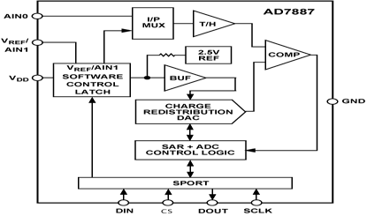
通过片内控制寄存器可将AD7887配置为单通道或双通道工作模式。在默认的单通道模式下,AD7887可作为只读ADC工作。以单通道模式工作时,存在一个模拟输入(AIN0),并且AIN1/V REF引脚用作V REF功能。通过此V REF引脚,用户可使用内部的2.5 V基准电压,或者将外部基准电压加载至此V REF引脚,为器件提供基准电压。外部基准电压的范围为2.5 V至V DD,AIN0上的模拟输入范围为0至V REF。
以双通道模式工作时,AIN1/VREF引脚用作AIN1功能,以便提供第二个模拟输入通道。这种情况下,器件的基准电压通过VDD引脚提供,因此,AIN0和AIN1上的模拟输入范围均为0至VDD。
CMOS结构可确保获得低功耗,正常工作模式下的典型功耗为2 mW,省电模式下为3 uW。该器件提供8引脚、0.15英寸宽窄体SOIC和8引脚MSOP两种封装。
The AD7887 is a high speed, low power, 12-bit analog-to-digital converter (ADC) that operates from a single 2.7 V to 5.25 V power supply. The AD7887 is capable of 125 kSPS throughput rate. The input track-and-hold acquires a signal in 500 ns and features a single-ended sampling scheme. The output coding for the AD7887 is straight binary, and the part is capable of converting full power signals of up to 2.5 MHz.
The AD7887 can be configured for either dual- or single-channel operation via the on-chip control register. There is a default single-channel mode that allows the AD7887 to be operated as a read-only ADC. In single-channel operation, there is one analog input (AIN0) and the AIN1/VREF pin assumes its VREF function. This VREF pin allows the user access to the part's internal 2.5 V reference, or the VREF pin can be overdriven by an external reference to provide the reference voltage for the part. This external reference voltage has a range of 2.5 V to VDD. The analog input range on AIN0 is 0 to VREF.
In dual-channel operation, the AIN1/VREF pin assumes its AIN1 function, providing a second analog input channel. In this case, the reference voltage for the part is provided via the VDD pin. As a result, the input voltage range on both the AIN0 and AIN1 inputs is 0 to VDD.
CMOS construction ensures low power dissipation of typically 2 mW for normal operation and 3 uW in power-down mode. The part is available in an 8-lead, 0.15-inch-wide narrow body SOIC and an 8-lead MSOP package.
AD7887 特性
- Specified for VDD of 2.7 V to 5.25 V
- Flexible power/throughput rate management
- Shutdown mode: 1 uA max
- One or two single-ended inputs
- Serial interface: SPI(R)/QSPITM/MICROWIRETM/DSP compatible
- 8-lead narrow SOIC and MSOP packages
- 额定电压(VDD):2.7 V至5.25 V
- 灵活的功耗/吞吐量管理
- 关断模式:最大1 uA
- 1个或2个单端输入
- 串行接口:SPI(R)/QSPITM/MICROWIRETM/DSP兼容
- 8引脚窄体SOIC和MSOP封装
AD7887 技术指标
- Resolution (Bits): 12bit
- # Chan: 2
- Sample Rate: 125kSPS
- Interface: Ser,SPI
- Analog Input Type: SE-Uni
- Ain Range: Uni (Vref)
- ADC Architecture: SAR
- Pkg Type: SOIC,SOP
AD7887 亮点
- Smallest 12-bit dual-/single-channel ADC; 8-lead MSOP package.
- Lowest power 12-bit dual-/single-channel ADC.
- Flexible power management options, including automatic power-down after conversion.
- Read-only ADC capability.
- Analog input range from 0 V to VREF.
- Versatile serial input/output port (SPI(R)/QSPITM/MICROWIRETM/DSP compatible).
- 最小的12位单/双通道ADC;8引脚MSOP封装。
- 功耗最低的12位单/双通道ADC。
- 灵活的功耗管理选项,包括转换后自动关断功能。
- 只读ADC功能。
- 模拟输入范围:0 V至VREF。
- (SPI(R)/QSPITM/MICROWIRETM/DSP兼容)。
AD7887 应用领域
- 电池供电系统(个人数字助理、医疗仪器、移动通信)
- 仪表和控制系统
- 高速调制解调器
AD7887 功能框图
AD7887 芯片订购指南
| 产品型号 | 产品状态 | 封装 | 引脚 | 温度范围 |
|---|---|---|---|---|
| AD7887AR | 量产 | 8 ld SOIC | 8 | 工业 |
| AD7887AR-REEL7 | 量产 | 8 ld SOIC | 8 | 工业 |
| AD7887ARM | 量产 | 8 ld MSOP | 8 | 工业 |
| AD7887ARM-REEL7 | 量产 | 8 ld MSOP | 8 | 工业 |
| AD7887ARMZ | 量产 | 8 ld MSOP | 8 | 工业 |
| AD7887ARMZ-REEL | 量产 | 8 ld MSOP | 8 | 工业 |
| AD7887ARMZ-REEL7 | 量产 | 8 ld MSOP | 8 | 工业 |
| AD7887ARZ | 量产 | 8 ld SOIC | 8 | 工业 |
| AD7887ARZ-REEL | 量产 | 8 ld SOIC | 8 | 工业 |
| AD7887ARZ-REEL7 | 量产 | 8 ld SOIC | 8 | 工业 |
| AD7887BR | 量产 | 8 ld SOIC | 8 | 工业 |
| AD7887BR-REEL | 量产 | 8 ld SOIC | 8 | 工业 |
| AD7887BR-REEL7 | 量产 | 8 ld SOIC | 8 | 工业 |
| AD7887BRZ | 量产 | 8 ld SOIC | 8 | 工业 |
| AD7887BRZ-REEL | 量产 | 8 ld SOIC | 8 | 工业 |
| AD7887BRZ-REEL7 | 量产 | 8 ld SOIC | 8 | 工业 |
| AD7887WARMZ | 量产 | 8 ld SOIC | 8 | 工业 |
| EVAL-AD7887CB | 量产 | 评估板 | - | 待定 |
AD7887 应用技术支持与电子电路设计开发资源下载
- AD7887 数据手册DataSheet下载 .PDF
- Analog Devices, Inc.ADI 美国模拟器件公司产品订购手册 .PDF
- ADC模数转换器选型指南 . PDF