AD7799: 3通道、低噪声、低功耗、24位Σ-Δ型ADC,内置片内仪表放大器
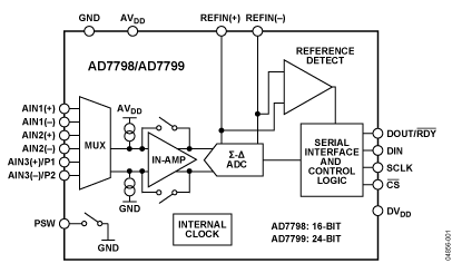
AD7798/AD7799均为适合高精度测量应用的低功耗、低噪声、完整模拟前端,内置一个低噪声16位/24位Σ-Δ型ADC,其中含有3个差分模拟输入,还集成了片内低噪声仪表放大器,因而可直接输入小信号。当增益设置为64、更新速率为4.17 Hz时,AD7799的均方根(RMS)噪声为27 nV,AD7798的均方根(RMS)噪声为40 nV。AD7798/AD7799片内特性包括一个低端电源开关、基准电压检测、可编程数字输出引脚、熔断电流控制和一个内部时钟振荡器。输出数据速率可通过软件编程设置,可在4.17 Hz至470 Hz的范围内变化。AD7798/AD7799采用2.7 V至5.25 V电源供电,AD7798的典型功耗为300 µA,而AD7799的典型功耗为380 µA,两款器件均采用16引脚TSSOP封装。
The AD7798/AD7799 are low power, low noise, complete analog front ends for high precision measurement applications. The AD7798/AD7799 contains a low noise, 16-/24-bit Σ-Δ ADC with three differential analog inputs. The on-chip, low noise instrumentation amplifier means that signals of small amplitude can be interfaced directly to the ADC. With a gain setting of 64, the rms noise is 27 nV for the AD7799 and 40 nV for the AD7798 when the update rate equals 4.17 Hz.
On-chip features include a low-side power switch, reference detect, programmable digital output pins, burnout currents, and an internal clock oscillator. The output data rate from the part is software-programmable and can be varied from 4.17 Hz to 470 Hz.
The part operates with a power supply from 2.7 V to 5.25 V. The AD7798 consumes a current of 300 μA typical, whereas the AD7799 consumes 380 μA typical. Both devices are housed in a 16-lead TSSOP package.
AD7799 特点
- 均方根(RMS)噪声:
27 nV(4.17 Hz、AD7799)
65 nV(16.7 Hz、AD7799)
40 nV(4.17 Hz、AD7798)
85 nV(16.7 Hz、AD7798) - 功耗:380 µA(典型值)
- 省电模式:最大1 µA
- 低噪声可编程增益仪表放大器
- 更新速率:4.17 Hz至470 Hz;3个差分输入
- 内部时钟振荡器
- 50 Hz/60 Hz同时抑制
- 基准电压检测
- 低端电源开关
- 可编程数字输出
- 熔断电流控制
- 电源电压:2.7 V至5.25 V
- RMS noise:
27 nV at 4.17 Hz (AD7799)
65 nV at 16.7 Hz (AD7799)
40 nV at 4.17 Hz (AD7798)
85 nV at 16.7 Hz (AD7798) - Current: 380 μA typical
- Power-down: 1 μA maximum
- Low noise, programmable gain, instrumentation amp
- Update rate: 4.17 Hz to 470 Hz 3 differential inputs
- Internal clock oscillator
- Simultaneous 50 Hz/60 Hz rejection
- Reference detect
- Low-side power switch
- Programmable digital outputs
- Burnout currents
- Power supply: 2.7 V to 5.25 V
AD7799 技术指标
- Resolution (Bits): 24bit
- # Chan: 3
- Sample Rate: n/a
- Interface: Ser,SPI
- Analog Input Type: Diff-Uni
- Ain Range: (2Vref/PGA Gain) p-p
- ADC Architecture: Sigma-Delta
- Pkg Type: SOP
AD7799 应用领域
- 电子秤
- 压力测量
- 应变计传感器
- 气体分析
- 工业过程控制
- 仪器仪表
- 便携式仪器仪表
- 血液分析
- 智能发射机
- 液体/气体色谱6位DVM
- Weigh scales
- Pressure measurement
- Strain gauge transducers
- Gas analysis
- Industrial process control
- Instrumentation
- Portable instrumentation
- Blood analysis
- Smart transmitters
- Liquid/gas chromotography 6-digit DVM
AD7799 建议配套产品
- Recommended References for the AD7799
- Recommended Precision Amplifiers for the AD7799
- Recommended Power Solutions
- For selecting voltage regulator products, use ADIsimPower.
- For selecting supervisor products, use the Supervisor Parametric Search.
AD7799 功能框图
AD7799 产品选型
| 产品型号 | 产品状态 | 封装 | 引脚 | 温度范围 |
|---|---|---|---|---|
| AD7799BRU | Prodn | 16 ld TSSOP | 16 | 工业 |
| AD7799BRU-REEL | Prodn | 16 ld TSSOP | 16 | 工业 |
| AD7799BRUZ | Prodn | 16 ld TSSOP | 16 | 工业 |
| AD7799BRUZ-REEL | Prodn | 16 ld TSSOP | 16 | 工业 |
| EVAL-AD7799EBZ | Prodn | EVALUATION BOARDS | - | 待定 |