AD549: Ultralow Input-Bias Current Operational Amplifier
The AD549* is a monolithic electrometer operational amplifier with very low input bias current. Input offset voltage and input offset voltage drift are laser trimmed for precision performance. The part’s ultralow input current is achieved with “Topgate” JFET technology, a process development exclusive to Analog Devices, Inc. This technology allows fabrication of extremely low input current JFETs compatible with a standard junction isolated bipolar process. The 1015 Ω common-mode impedance, which results from the bootstrapped input stage, ensures that the input current is essentially independent of common-mode voltage.
The AD549 is suited for applications that require very low input current and low input offset voltage. It excels as a preamp for a wide variety of current output transducers, such as photo-diodes, photomultiplier tubes, or oxygen sensors. The AD549 can also be used as a precision integrator or low droop sample and hold. The AD549 is pin compatible with standard FET and electrometer op amps, allowing designers to upgrade the performance of present systems at little additional cost.
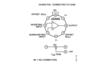
The AD549 is available in a TO-99 hermetic package. The case is connected to Pin 8 so that the metal case can be independently connected to a point at the same potential as the input terminals, minimizing stray leakage to the case. The AD549 is available in four performance grades. The J, K, and L versions are rated over the commercial temperature range of 0°C to +70°C. The S grade is specified over the military temperature range of -55°C to +125°C and is available processed to MIL-STD-883B, Rev. C. Extended reliability plus screening is also available. Plus screening includes 168 hour burn-in, as well as other environmental and physical tests derived from MIL-STD-883B, Rev. C.
产品焦点 Product Highlights
- The AD549 input currents are specified, 100% tested, and guaranteed after the device is warmed up. They are guaranteed over the entire common-mode input voltage range.
- The AD549 input offset voltage and drift are laser trim-med to 0.25 mV and 5 μV/°C (AD549K), and to 1 mV and 20 μV/°C (AD549J).
- A maximum quiescent supply current of 700 μA minimizes heating effects on input current and offset voltage.
- AC specifications include 1 MHz unity gain bandwidth and 3 V/μs slew rate. Settling time for a 10 V input step is 5 μs to 0.01%.
产品应用领域 Applications
- Electrometer amplifier
- Photodiode preamp
- pH electrode buffer
- Vacuum ion gauge measurement
AD549 特点
- Ultralow input-bias current
- 60 fA maximum (AD549L)
- 250 fA maximum (AD549J)
- 60 fA maximum (AD549L)
- Input-bias current guaranteed over common-mode voltage range
- Low offset voltage
- 0.25 mV maximum (AD549K)
- 1.00 mV maximum (AD549J)
- 0.25 mV maximum (AD549K)
- Low offset drift
- 5 μV/°C maximum (AD549K)
- 20 μV/°C maximum (AD549J)
- 5 μV/°C maximum (AD549K)
- Low power
- 700 μA maximum supply current
- Low input voltage noise
- 700 μA maximum supply current
- 4 μV p-p 0.1 Hz to 10 Hz
- MIL-STD-883B parts available
AD549 功能框图
AD549 技术指标
| -3dB Bandwidth | 1MHz | Vcc-Vee Supply (V) | 10 to 36 |
| Slew Rate | 3V/us | Iq per Amplifier | 700uA |
| Vos | 500uV | # OpAmps per Pkg | 1 |
| Ib | 150fA | Operating Temp Range | 0 to +70 |
| Input Noise (nV/rtHz) | 35nV/rtHz | Packages | TO-X |
AD549 订购指南
| 产品型号 | 产品状态 | 封装 | 引脚 | 温度范围 |
|---|---|---|---|---|
| AD549JH | 量产 | 8 ld Header | 8 | 商业 |
| AD549JHZ | 量产 | 8 ld Header | 8 | 商业 |
| AD549KH | 量产 | 8 ld Header | 8 | 商业 |
| AD549KHZ | 量产 | 8 ld Header | 8 | 商业 |
| AD549LH | 量产 | 8 ld Header | 8 | 商业 |
| AD549LHZ | 量产 | 8 ld Header | 8 | 商业 |
| AD549SH/883B | 量产 | 8 ld Header | 8 | 军用 |