AD524: 仪表放大器
The AD524 is a precision monolithic instrumentation amplifier designed for data acquisition applications requiring high accuracy under worst-case operating conditions. An outstanding combination of high linearity, high common mode rejection, low offset voltage drift, and low noise makes the AD524 suitable for use in many data acquisition systems.
The AD524 has an output offset voltage drift of less than 25 uV/ °C, input offset voltage drift of less than 0.5 uV/°C, CMR above 90 dB at unity gain (120 dB at G = 1000) and maximum nonlinearity of 0.003% at G = 1. In addition to the outstanding dc specifications the AD524 also has a 25MHz gain bandwidth product (G = 1000). To make it suitable for high speed data ac-quisition systems the AD524 has an output slew rate of 5 V/us and settles in 15us to 0.01% for gains of 1 to 100.
As a complete amplifier the AD524 does not require any external components for fixed gains of 1, 10, 100 and 1,000. For other gain settings between 1 and 1000 only a single resistor is required. The AD524 input is fully protected for both power on and power off fault conditions.
The AD524 IC instrumentation amplifier is available in four different versions of accuracy and operating temperature range. The economical "A" grade, the low drift "B" grade and lower drift, higher linearity "C" grade are specified from -25°C to +85°C. The "S" grade guarantees performance to specification over the extended temperature range -55°C to +125°C. Devices are available in 16-pin ceramic DIP and SOIC packages and a 20-terminal leadless chip carrier.
产品应用领域 Applications
- The AD524 has guaranteed low offset voltage, offset voltage drift, and low noise for precision high gain applications.
- The AD524 is functionally complete with pin program- mable gains of 1, 10, 100, and 1000, and single resistor programmable for any gain.
- Input and output offset nulling terminals are provided for very high precision applications and to minimize offset voltage changes in gain ranging applications.
- The AD524 is input protected for both power-on and power-off fault conditions.
- The AD524 offers superior dynamic performance with a gain bandwidth product of 25 MHz, full power response of 75 kHz and a settling time of 15 μs to 0.01% of a 20 V step (G = 100).
AD524 特点
- FeaturesLow Noise: 0.3 uV p-p 0.1 Hz to 10 Hz
- Low Nonlinearity: 0.003% (G = 1)
- High CMRR: 120 dB (G = 1000)
- Low Offset Voltage: 50 uV
- Low Offset Voltage Drift: 0.5 uV/°C
- Gain Bandwidth Product: 25 MHz
- Available in tape and reel in accordance with EIA-481A
- Pin Programmable Gains of 1, 10, 100, 1000
- Input Protection, Power On–Power Off
- No External Components Required
- Internally Compensated
- MIL-STD-883B and Chips Available
- 16-lead ceramic DIP and SOIC packages and 20-terminal leadless chip carrieravailable
- Standard military drawing also available
AD524 功能框图
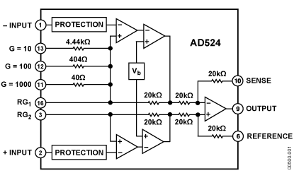
AD524 功能框图
AD524 技术指标
| Single/Dual Supply | Dual | Vnoise RTI 1-10 Hz uVp-p | 0.3uV p-p |
| Voltage Supply (Vmax) | ±18V | Temperature Range | -55 to +125 |
| Gain Setting Method | Pin | Gain Error (%) max | ±0.25% |
| Gain Range (min to max) | 1000 | Supply Current | 5mA |
| Bandwidth G=10 (kHz typ) | 400kHz | Vosi (uV) | 250uV |
| CMRR (dB) | 90dB |
AD524 订购指南
| 产品型号 | 产品状态 | 封装 | 引脚 | 温度范围 |
|---|---|---|---|---|
| 5962-8853901EA | 量产 | 16 ld Side-Brazed CerDIP | 16 | 军用 |
| AD524AD | 量产 | 16 ld Side-Brazed CerDIP | 16 | 工业 |
| AD524ADZ | 量产 | 16 ld Side-Brazed CerDIP | 16 | 工业 |
| AD524AE | 量产 | 20 ld LCC | 20 | 工业 |
| AD524AR-16 | 量产 | 16 ld SOIC - Wide | 16 | 工业 |
| AD524AR-16-REEL | 量产 | 16 ld SOIC - Wide | 16 | 工业 |
| AD524AR-16-REEL7 | 量产 | 16 ld SOIC - Wide | 16 | 工业 |
| AD524ARZ-16 | 量产 | 16 ld SOIC - Wide | 16 | 工业 |
| AD524ARZ-16-REEL7 | 量产 | 16 ld SOIC - Wide | 16 | 工业 |
| AD524BD | 量产 | 16 ld Side-Brazed CerDIP | 16 | 工业 |
| AD524BDZ | 量产 | 16 ld Side-Brazed CerDIP | 16 | 工业 |
| AD524BE | 量产 | 20 ld LCC | 20 | 工业 |
| AD524CD | 量产 | 16 ld Side-Brazed CerDIP | 16 | 工业 |
| AD524CDZ | 量产 | 16 ld Side-Brazed CerDIP | 16 | 工业 |
| AD524SD | 量产 | 16 ld Side-Brazed CerDIP | 16 | 军用 |
| AD524SD/883B | 量产 | 16 ld Side-Brazed CerDIP | 16 | 军用 |
| AD524SE/883B | 量产 | 20 ld LCC | 20 | 军用 |
AD524 应用技术支持与电子电路设计开发资源下载
- 差分放大器系列AD524 数据手册DataSheet 下载 . PDF
- ADI 模拟器件公司比较器产品选型指南 . PDF
- 仪表放大器设计者指南(第三版) . PDF
- Analog Devices, Inc. 美国模拟器件公司产品订购手册 .PDF